
 admin
adminDesigns for HDI PCBs
A PCB is an intricate and vital part of almost all electronic devices. It’s also a complex piece of engineering, and it requires proper design for the optimal function and reliability of your product. Whether you’re designing an analog or digital circuit, there are many considerations that come into play when creating a PCB. For example, you want to ensure that the different components aren’t interfering with one another or sending signals at inappropriate frequencies. Additionally, you need to ensure that the grounding is adequate for your device’s specific needs.
When working with mixed-signal designs in HDI PCBs, there are some unique considerations that you need to take into account. To start with, you’ll need to ensure that the grounding is adequate to avoid interference between the analog and digital sections of your device. Additionally, you’ll need to ensure that signal paths are short and direct in order to minimize inductance and maintain high-speed performance. Finally, you’ll need to ensure that the power supply traces are isolated from analog and digital systems in order to prevent crosstalk.
An HDI PCB, or high density interconnect PCB, is a multi-layer printed circuit board that offers more space and higher component density than traditional single- or double-sided PCBs. This technology allows designers to incorporate more components on a smaller board with better signal integrity, while using the latest manufacturing techniques, including fine-pitch solder masks and advanced materials.
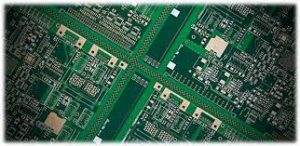
Mixed-Signal Designs in HDI PCBs
The HDI technology used in these PCBs also allows for a more efficient manufacturing process, reducing assembly steps and costs. This is because HDI boards can be made with either blind or buried vias, and offer more connection pad density than conventional PCBs. Additionally, the smaller trace and spacing widths of HDI PCBs allow for more efficient routing and reduced interference between components.
While the benefits of working with an HDI PCB are obvious, it’s important to keep in mind that these circuits are more complicated than their traditional counterparts. The increased layer count can result in additional assembly steps and higher production costs, but you can reduce these costs by choosing a shorter turnaround time from your PCB supplier.
When choosing a PCB manufacturer, be sure to choose a partner with a fast turnaround time and customer service that is quick to respond to questions or concerns. This will help to keep your costs down and make the process more efficient, which will increase your cost-effectiveness.
When it comes to designing an HDI PCB, you should always keep in mind the same design rules that apply when working with a traditional PCB. For example, you should aim to use the minimum number of layers possible, as this can significantly reduce your assembly costs. You should also make sure to follow your designer’s recommendations for component placement, as this will be more accurate than relying on your own intuition. Additionally, you should be wary of putting too much copper in your board, as this can add to the overall cost.
