
 admin
adminPCB Manufacturers Assist in Reducing Signal Degradation
A circuit board is a multilayered platform that houses an intricate network of electrical pathways. These pathways, made of copper, allow current to flow between different components and ensure that signals reach their intended destinations without interference or distortion. The future of circuit boards looks promising, with advancements aligning with the demands of emerging technologies. With the rise of artificial intelligence, quantum computing, and the Internet of Things (IoT), circuit boards must evolve to meet higher performance and efficiency standards.
While these conductive pathways are essential to the functioning of a circuit board, they’re also vulnerable to various factors that can compromise their performance and reliability. Fortunately, PCB manufacturers can assist in the prevention of signal degradation through a variety of design and manufacturing techniques.
The first step in creating a circuit board circuit board is designing a schematic, which is a detailed description of the parts and connections that make up the overall circuit. Typically drawn on graph paper or using computer-aided design (CAD) software, the schematic provides a clear and easy-to-follow guide for how the board is to be constructed. However, even with a carefully designed schematic, there are many ways that a circuit board can fail to function properly.
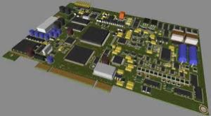
How PCB Manufacturers Assist in Reducing Signal Degradation
Poor PCB Construction One of the most common causes of signal degradation in a circuit board is poor workmanship during the fabrication process. This can include misalignments between layers, traces that are too long or thin, and the presence of copper where it shouldn’t be. It can also result in a lack of proper soldering, which can cause unintended connections and shorts between components.
Another source of signal degradation is impedance discontinuities that can produce reflections. This occurs when a transmission line and load have incompatible impedances, causing energy to disperse over the circuit board and interfere with signal propagation. Impedance matching techniques such as series, parallel, and Thevenin termination can reduce this problem by minimizing reflections.
Other sources of signal degradation include jitter, noise coupling, and power supply issues. Jitter can increase the delay between a signal’s rising and falling edges, degrading its quality and leading to data errors. Noise coupling is made worse by the use of longer traces and vias, which can be used as an antenna to broadcast unwanted electromagnetic interference (EMI). EMI issues are mitigated through the use of a ground plane and proper stack-up design.
A final common cause of signal degradation in a circuit board is the presence of plating voids. These voids occur when imperfections in the deposition process of a thru-hole prevent an electrical current from passing through it. This can lead to faulty connections and a breakdown of the circuit board. Fortunately, this can be prevented by selecting the right materials and deposition process for each application. It’s also crucial to choose a manufacturing company with a good reputation and extensive experience. This will help to ensure that the quality of your product is consistent.

